
UV exposure box
I used to make my own circuits with the toner transfer method. However, it has a lot of drawbacks, especially for SMD components with fine pitch. The first step to high resolution PCBs is building my own ultraviolet exposure box.
Instead of using UV tubes, I’ve made an array of UV leds. They are cheaper, more durable and energy efficient. These are the features:
– exposure area of 18×24 cm
– 2 boards of 54 leds each, in 6×9 configuration. 108 leds in total.
– 2 cm of separation between each pair of leds, 7 cm between the leds and the PCB.
– twin led array configuration for a white light box (to align transparencies).
– exposure time: not critical, 6 to 11 minutes
Electronics
The measured forward voltage of the leds is 3.27 volts. They are configured in series of 3 leds with a resistor of 120 ohms, which gives a current of 18.5 mA when using a 12 volts power supply.
LED PCB
The PCBs for the led matrix has been made with the toner transfer method. The huge size of the boards used (180×120 mm) cools down the laminator and the toner didn’t stick well to the copper, so I had to use a pen marker. This is one of the reasons I’m going for the UV exposure method.
Note that there are in fact two circuits in the board. One is for the UV leds and the other is for the white leds (which I haven’t received yet). Thus, half of the holes will remain unpopulated for the moment.
![]()
After soldering the resistors and the leds, I filed and sanded them flat to help diffusing the light emitted (originally at 20º). A pair of marker pens were cut and placed at the sides of the two PCBs in order to hold them together. It’s a fast and clean way to keep them in position while I receive the white leds.

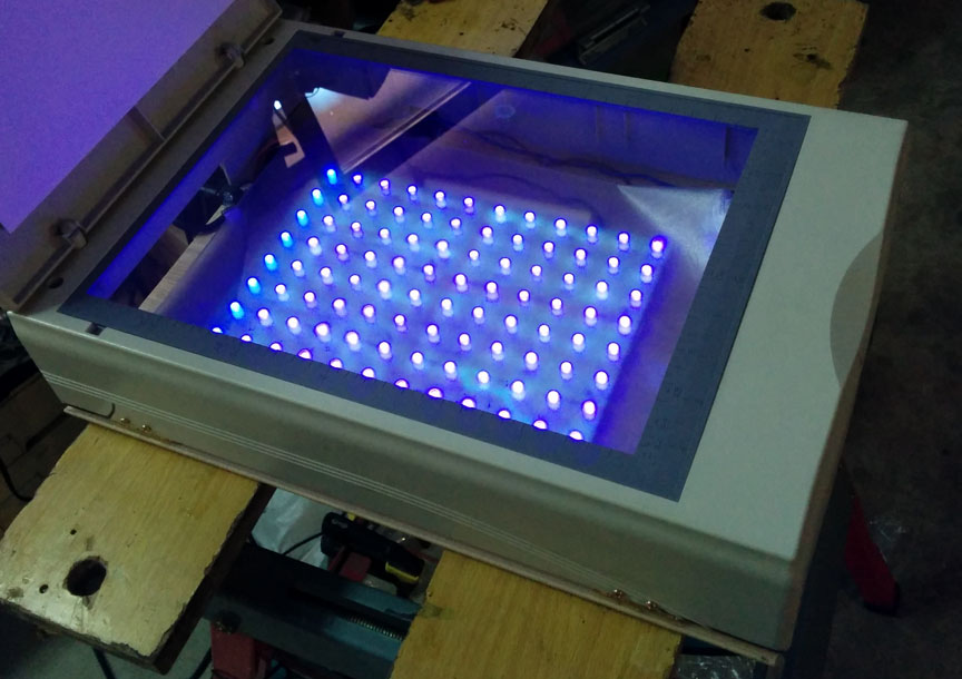
I put the circuit inside an old scanner, and tested the leds for dead units. Note the old halogen lamp which will be removed as soon as I get the white leds.

I used a translucid plastic sleeve as a light diffuser.

And this is the light pattern, pretty homogeneous in my opinion.

Testing the exposure box
A lot of parameters are involved in the ideal exposure time of a specific photosensitized board: number of leds, distance to the leds, etc. Having other exposure box as a referenced, I estimated the times to be between 3 and 10 minutes. To find the best time of my setup, I designed a board with traces from 0.01′ width (0.254 mm) to 0.05′ (1.270 mm) and clearing spaces from 0.254′ to 0.635′. The circuit was replicated four times, so that each one of them could be exposed to UV for a different period of time (3, 6, 9 and 11 minutes).
I printed the four identical circuits two times in a transparency with a laser printer, and folded them together to get deeper blacks.
![]()
This was the result after revealing the PCB.

Three of them seem to be very similar, which were exposed to 6, 9 and 11 minutes of UV ligth. The darkest one was exposed 3 minutes. Let’s go and etch them.

I was surprised of the high resolution achieved. The results are fairly consistent despite the different exposure times used. The least exposed one (botton-left) needed a longer etching process, but I stopped it to avoid damaging the others. Here is the result after cleaning the PCB.

This is the detail of the 9 minutes one:

And these are the thinnest tracks seen under the microscope.
Still room for even thinner traces in my opinion!
Update:
The project files have been uploaded to Github.